Mask Layout Design Rules
Layout And Mask Conventions
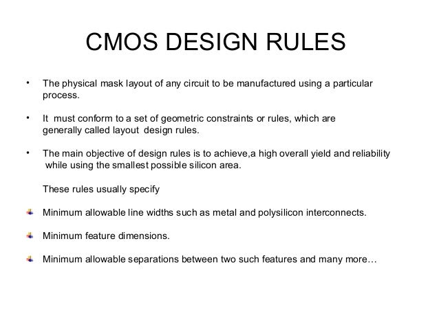
Cmos Design Rule

Vlsi Design Lecture 2 Basic Fabrication Steps And Layout Ppt

Design Of Vlsi Systems Chapter 3
Http Www Inst Eecs Berkeley Edu Ee143 Fa10 Lectures Lec 20 Pdf

Introduction To Layout Design Rules

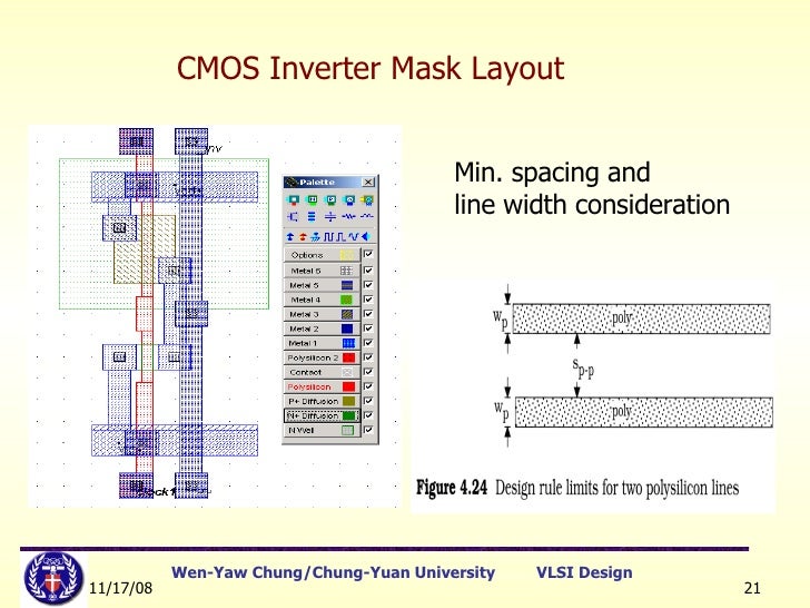
The mask design rules for this process are a mix of 0 25 µm and 0 5 µm.
Mask layout design rules. If you must have data outside of the mask area such as a title border make sure it is on a separate layer and purge that layer prior to running a translation to dxf. Covers design rules and techniques to draw the layout of any design of nmos pmos or cmos. The most important parameter used in design rules is the minimum line width. The physical mask layout design of cmos logic gates is an iterative process which starts with the circuit topology and the initial sizing of the transistors.
N type diffusion in p wells define nmos transistors. N implant mask defines areas where n type diffusion is required. Transistor is designed with at least for masks. P type diffusion in n wells defines pmos transistors.
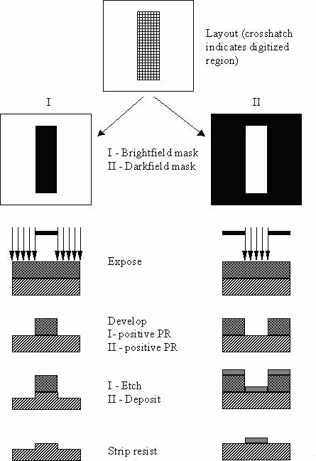
Design rules are consisting of the minimum width and minimum spacing requirements between objects on the different layers. Avoid drawing your mask so that it is far away from the origin c this could cause problems later on. When a mask is printed from the computer generated layout the user typically has the option of having the features on the layout printed in lightfield or darkfield polarities as shown in figure 19. Active mask defines where p or n diffusion type or gates will be placed.
It is necessary to select the polarity to achieve the desired resist image on the wafer depending on whether a subtractive or additive process will pattern the underlying layer and the polarity. 3 2 cmos layout design rules as already discussed in chapter 2 each mask layout design must conform to a set of layout design rules which dictate the geometrical constraints imposed upon the mask layers by the technology and by the fabrication process. It is extremely imporant that the layout design must not. But before we present the options let s go over the basics of mask design.
For all the remaining layers including collector resistor capacitor wire via and pad 0 5 µm design rules should be used. The layout designer must follow these rules in order. Protecting yourself versus protecting others the pattern you choose will depend on your reason for wearing a mask. The layout design rules provide a set of guidelines for constructing the various masks needed in the fabrication of integrated circuits.
Do not draw any data outside of the normal extents of your mask. Many manufacturers has a pcb design rules file for eagle ready to be downloaded so that you only need to load it into eagle. Also the color codes and design encoding to follow.

Layout Design Rules 2 Introduction Layout Rules Is Also
Https Nptel Ac In Content Storage2 Courses 117101058 Downloads Lec 13 Pdf
Ic Layout Mask Design Youtube

Electronic Systems 2015 Cmos Design Rules Youtube
Layouts

Module 3 Mos Designs Stick Diagrams Designrules Ppt Video
Http Users Encs Concordia Ca Asim Coen 20451 Lectures W 9 W9 Overview Pdf
Lect5 Stick Diagram Layout Rules

Vlsi Concepts November 2014
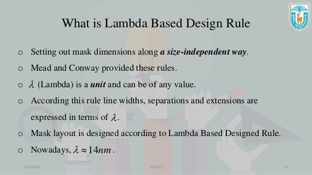
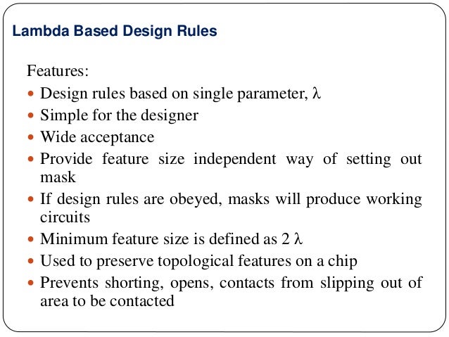
Stick Diagram And Lambda Based Design Rules
Https Labs Ece Uw Edu Cam Tutorials Maskdesign Pdf
The Five Challenges Of Sub 28nm Custom Ic Design

About Nazca Design